The PCB layout is printed on a glossy paper sheet using a black and white laser printer. Printing parameters are set to "darkest" to get the thickest and darkest result.
Toner ink is then transfered on the copper clad. To do that, the ink is heated to 190°C and then pressed on the clad. The copper is previously sanded with very fine sand paper (800 grade) and finally cleaned with aceton.
I have used a laminator to heat the clad and achieve a clean transfer.
The paper is separated from the toner using very hot water.
The laminator must be modified to increase it's temperature to 190°C.
We will see how to do that easily and with a very limited budget (less than 40€). But before, launch your player and look at this video to be fully convinced of the simplicity of this process.
Laminator modification
I used a Smart model from GBC. The following mods are well fitted to this model but should probably be adapted if you have another model.
It's rather straightforward :
Open the laminator,
Inside you'll see a yellow wire running under the rolls on the back side of the laminator.
You just have to cut this wire and put a 6.8k resistor in serie.
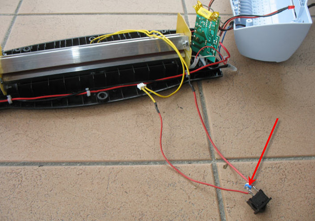
Practically I rather put a 10k potentiometer to have fine tuning possibility to adjust the temperature to 170°C when the green led is On.
You can notice that I have put the original power switch in parallel of the potentiometer. I can then use the laminator to its original function
Of course the 220V power is no longer cut by the switch. As soon as I power the plug... the laminator gets On.
Even the heathing off, the temperature climbs a bit up to 190°C. And it's perfect
For Brother laser printers you will have to increase the temperature up to 210°C as the toner is not the same as other brands (HP, Lexmark, ...)
I have been forced to correct a few anomalies... Plastics are melting...
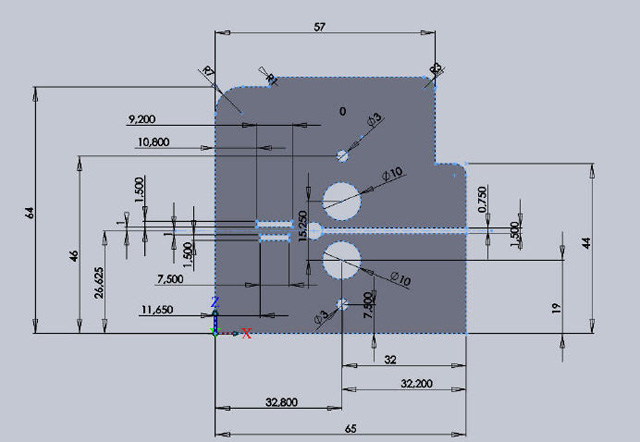
I have redesigned the rolls supports in epoxy and milled them with my CNC .
The pattern for the supports can be downloaded here : dxf format
Here is the result, you can see the new epoxy support.
Click on the vidéo you will see the "open laminator" digesting the copper clad.
A few precisions
copper clad is a simple one with no photoresist on it (cheaper)
paper is a glossy paper from a magazine "it's sticking a little with wet fingers " it looks nice but is very thin
PCB etching
It's time to etch your brand new PCB..
The method explained here after is very simple, rather clean, products can be stored years, and you see what you do (nice when you want to inspect if the etching process is finished...)
Only advantages
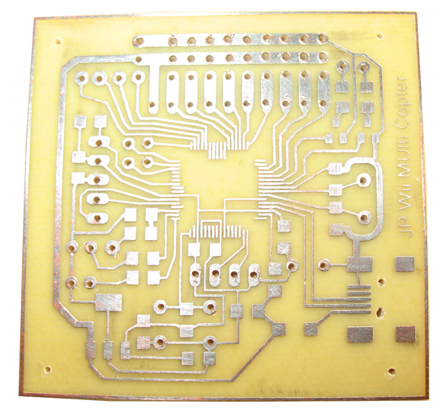
Finally the result will be perfect. I succeeded in etching 1/10mm wide tracks, printed with the toner transfer method and etched as follows.
On this example (real size 5cm * 5cm), the main componant is a PIC24FJ256GB106 MCU. The pads are 0,3mm wide and inter pads is 0,2mm.
To etch your board you will need 3 minutes and the following products :
chlorhydric acid (HCl).
water
hydrogen peroxide (H2O2 at 30%).
rubber gloves
protection glasses
ceramic or glass plate
Manipulating these product can be very dangerous. Use them at your own risk...
etch your PCBs in open space with enough air flow. (toxic chlorine gaz will be produced
wear gloves
wear protection glasses
mix products with the following proportions :
4 water volumes
1 hydrogen peroxide volume
1 acid volume
Always put acid into water and never the contrary...